
Development of n-GaAs/n-InP Wafer Bonding
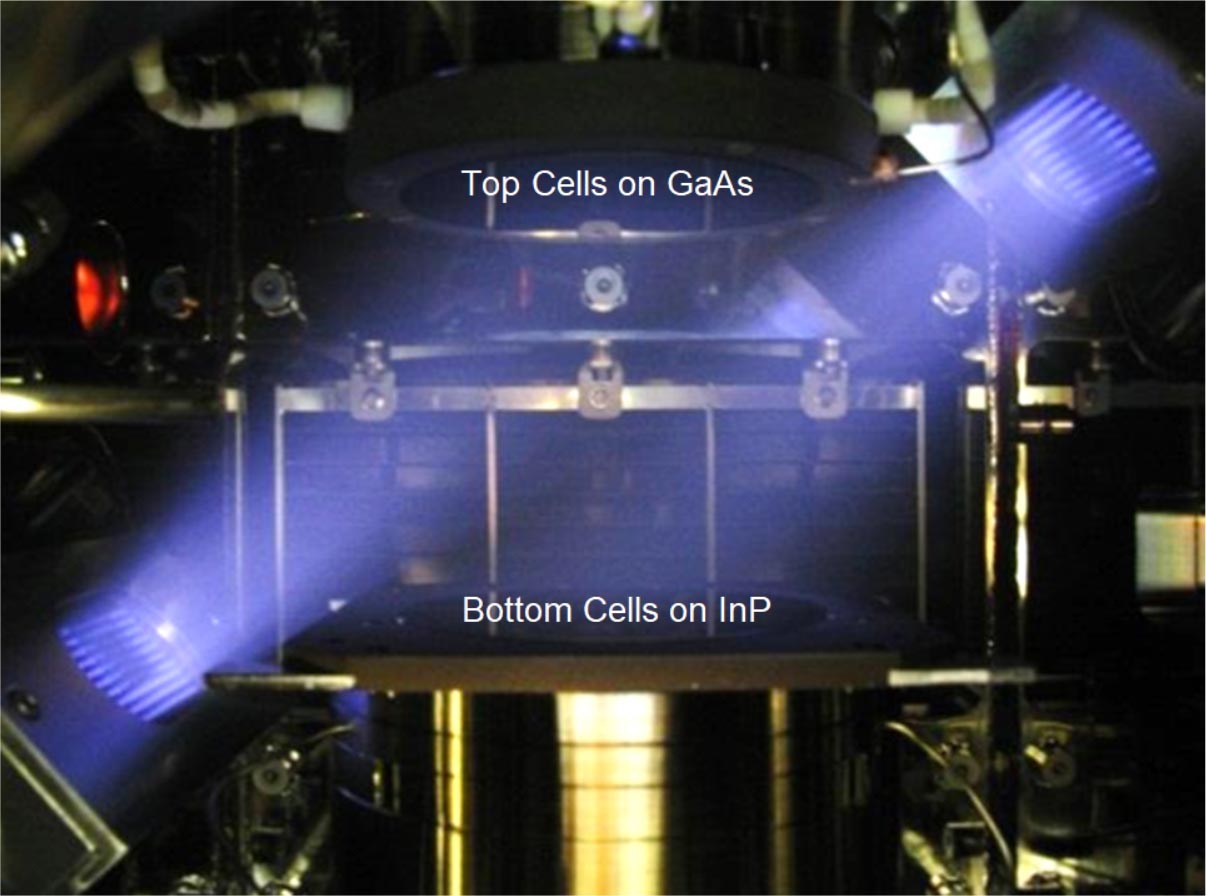
Argon-beam activated wafer bonding is a key process for the fabrication of the multi-junction solar cell in the “50 Prozent” project.
Here, the top cells grown on a GaAs and the bottom cells grown on InP are monolithically combined by a n-GaAs/n-InP heterojunction.
The process flow is as follows: the wafer surfaces are first polished by means of chemical-mechanical polishing in order to ensure smooth surfaces without any particles. Then the wafer surfaces are sputtered with Argon atoms in a vacuum to remove oxides (see photograph of the bond chamber), leaving dangling bonds on the surfaces.
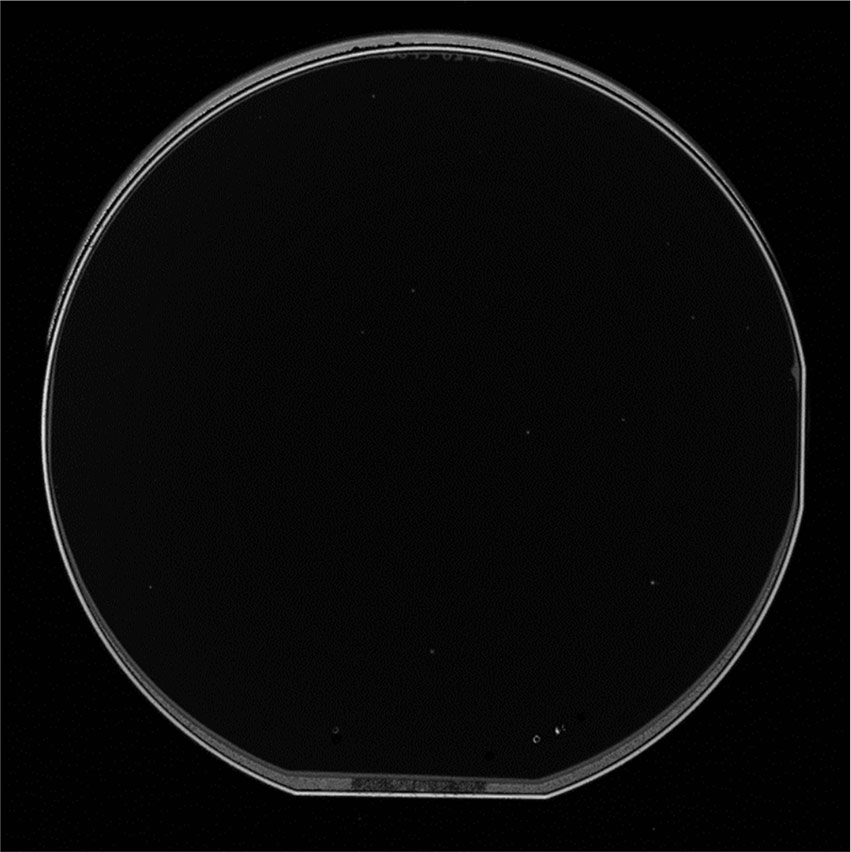
By pressing the wafers together, these dangling bonds form covalent bonds, permanently joining the semiconductors. The sputtering process for GaAs and InP was investigated in detail to ensure a complete oxide removal and avoid surface roughening at the same time. With optimized process parameters it was possible to fully combine the n-GaAs/n-InP heterojunction, as can be seen in the scanning-acoustic microscopy image. The non-bonded area at the edges of the bond can be correlated to the rounded bevel edge of the wafers. This result is the first important milestone in the realization of the targeted four- or six-junction solar cell at Fraunhofer ISE.